
Deep-learning enabled generalized inverse design of multi-port radio-frequency and sub-terahertz passives and integrated circuits

Utilizing the deep-learning enabled robust EM emulator that eliminates the need for time and resource intensive EM simulations, one can now conceive of rapid synthesis in the large design space of arbitrary structures and circuits with optimization algorithms (Fig. 1c). This can either be achieved through heuristic algorithms such as genetic algorithms (GA), simulated annealing or generative AI tools such as auto-encoders or tandem neural networks26. One can use the predictive model with a generative AI framework or with RL. We provide a more extensive comparison a the generative AI framework for synthesis in Supplementary Material Fig. S2.
Starting from a random structure, quick convergence to candidate solutions can be achieved through the evolution process. In this aspect, hyper-parameter choice for the GA is essential for ensuring exploratory strategy of the optimization loop. Firstly, we use a tournament selection method to determine the parents of each member of the next generation44. For a typical population size of M=4096, a tournament size of N=256 is adopted. As a result, population members with above average success have a decent chance for being selected as the parent. Upon parent selection and crossing over, each pixel has a mutation probability of flipping. This probability starts from 0.1 and vanishes to 0 towards the end of total number of iterations (100 in this paper). In addition, the best A=8 members of the current population are directly transferred to the next generation, guaranteeing a monotonous cost value reduction trajectory.
Figure 3 illustrates with several examples robust generalized inverse synthesis approach performed from single port antennas to multi-port EM structures based on the targeted scattering parameters; including one-port multi-band antennas, two-port bandpass filters, three-port power dividers with unique phase relationship, four-port resonant quadrature hybrid and three-port frequency diplexers. Figure 3a shows a packaged multi-band antenna (matched at 25 and 28 GHz) implemented in a compact area. In Fig. 3b, we show the synthesis of a band-pass two-port filter designed for 50-60 GHz, compressed to a size of λ/10 × λ/10 synthesized in a few minutes. For three ports, we demonstrate two complex design examples. In Fig. 3c, the input signal gets equally power split between two paths and maintain a 90∘ phase difference between the two paths at 60 GHz. The evolved EM structure achieves this almost exactly with nearly 0 dB amplitude difference, 1 dB insertion loss and 88∘ phase difference. In the second 3-port structure (Fig. 3e), we synthesize a diplexer that splits the single input into two paths depending on the frequency (similar to a wavelength division multiplexer). The lower band is 24–40 GHz and the upper band is 60–80 GHz. It can be seen that the method successfully achieves a diplexer with 2–4 dB insertion loss, and adjacent channel leakage less than -10 dB between 30-80 GHz, within an implemented area of λ/6 × λ/6 at the crossover frequency of 50 GHz. Figure 3d shows a 4-port EM structure with quadrature symmetry implementing a hybrid coupler.

a Inverse synthesis of multi-band packaged mm-Wave antenna operating at 24 and 28 GHz. b Inverse synthesis of a 2-port on-chip bandpass filter with a pass band target of 50-60 GHz. The filter (16 × 16 pixel, 300 × 300 μm) is compact with each side being λ/10 at 50 GHz. c Inverse synthesis of a 3-port equal power divider with ≈ 90∘ phase shift between 2 output ports at 60 GHz. d Inverse synthesis of a a 4-port 24 × 24 pixel quadrature hybrid between 70 and 80 GHz, showing close to ideal amplitude balance and phase relationship. e. Inverse synthesis of on-chip frequency diplexer (20 × 20 pixel 500 × 500 μm) with channel bandwidths of 24–40 GHz and 60–80 GHz.
We also demonstrate how the initial structure evolves to the final one to approach the desired performance. In Fig. 4a, we show how the frequency diplexer circuit evolves across optimization steps. The two frequency slices show the desirable performance where the signal flows to port 1 at 37 GHz (S31 = 1, S32 = 0), and it flips at 80 GHz (S31 = 0, S32 = 1). We can observe that initially most of the population is spread randomly, and as the generations evolve, the structures start to move towards the target points, finally leading to the structure that approaches the desired performance.

a Scatter plot showing the evolutionary progress of the frequency diplexer design progressing towards the ideal design point for 37 and 80 GHz. b, c Demonstration of generalized learning ability by the inverse synthesis method. We compare the inverse synthesis of two EM structures. The first one is an unequal power divider with a 4.7 dB power difference between the two output ports. The second one is an equal power divider with a bandpass filter response. In both cases, the synthesized structures (25 × 25 pixel 400 × 400 μm) demonstrate a better result than the best of the training data. This demonstrates the ability of the deep learning based model to generalize, and the inverse synthesis to successfully sample the design space.
Generalization ability of CNN
The EM emulator model needs to be able to predict structures that are not present in the dataset, such as those that can outperform structures present in the training data set. This is necessary for generalized inverse synthesis method. Figure 4 demonstrates this generalization ability as the inverse synthesis can tailor the structure to engineer the spectral response, distinctly different from what it has been trained with. The figure compares the results of structure that emerged through inverse synthesis and the best results from the training data for 2 different targets. Figure 4b shows the synthesis of a broadband uneven power divider that aims a power splitting ratio of 75%-25% across the bandwidth from 24 to 80 GHz. As it can be seen, the inverse design solution achieves better bandwidth, amplitude balance, and total transmission across 24-80 GHz, when compared to the best result from the training data. This demonstrates that the CNN model is not a lookup table, but is able to extract the relevant features that can robustly predict the scattering parameters of arbitrary structures, allowing the ability to search through this unexplored space during synthesis. Figure 4c shows a filtering power divider that performs equal power split and band pass filtering in each of the signal paths. Compared to the sample from the dataset, inverse design solution can provide a better trade-off between pass-band and stop-band requirements, while achieving near perfect amplitude and phase balance.
Furthermore, we can show that the initial computational cost for training dataset generation can be amortised very quickly by utilizing inverse design for different design goals. This was illustrated in detail in Fig. 5. When compared to the traditional EM simulation-based meta-heuristic methods, CNN aided inverse design can reduce design time to minutes from weeks, significantly reducing time and resource for synthesis. Moreover, once a model is trained it could be re-utilized for different design targets, which is in contrast to EM-based optimization where a new set of simulations needs to be performed at for different set of goals.
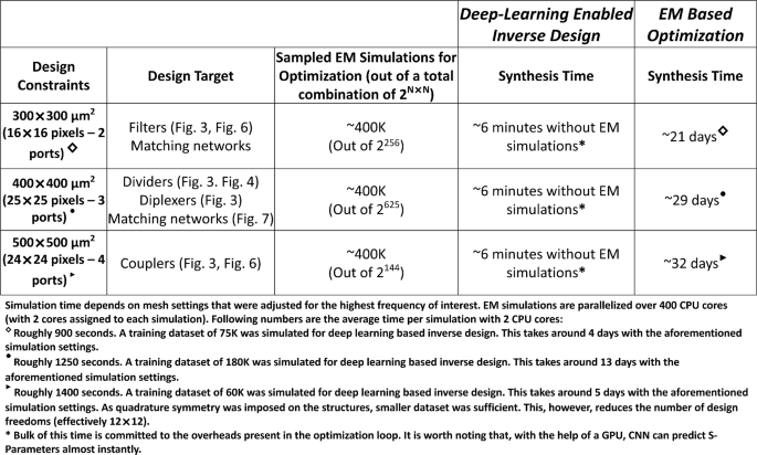
By removing the constraints of iterative EM simulations, the proposed method can drastically reduce the time of synthesis. Moreover, once a model trained, it can be utilized for different design goals and synthesize EM structures within minutes, which is in stark contrast with EM-based optimization.
Measurement results
To validate the generalized synthesis approach, we design, fabricate, and measure several examples of electromagnetic structures for mm-Wave frequencies, as well as an end-to-end broadband mm-Wave amplifier. All the electromagnetic structures and the mm-Wave amplifier are fabricated in industry standard bipolar complementary-oxide-metal-semiconductor (BiCMOS) process. The antennas are realized in a standard printed circuit board (PCB) process. We first present the results of two-port band-pass filter structures, and examine experimentally the effect of the size of the structure, number of pixels, and the results with different optimization algorithms, such as genetic algorithm (GA) and binary particle swam optimization (BPSO).
Size
The inverse synthesis can be guided to search for a compact structure that achieves a desired spectral response. Ultimately, this is limited by Maxwell’s laws. An electromagnetic structure effectively distributes electrical and magnetic energy within the structure to synthesize any spectral response. Therefore, the structure needs to be comparable to the wavelength to allow resonant-type behavior. Figure 6 captures this experimentally as we scale the structure from λ/12 × λ/12 (200 μm in each side) to λ/5 × λ/5 (500 μm in each side) across three step sizes, all implemented in the BiCMOS process. As can be seen in Fig. 6a, the spectral response can be seen to made broadband (covering 50-70 GHz) with flatter passband responses, due to more effective containment of the energy at 60 GHz with less leakage.

a Frequency response of two-port band-pass filters (16 × 16 pixel) with varying sizes including 200 × 200 (≈λ/13 each size), 300 × 300 (≈λ/8) and 500 × 500 μm (≈λ/5). Increasing the size increases the effective filter order resulting in broadband response as seen in the measurements. b Inverse-designed filters with varying pixel sizes between 10 × 10, 12 × 12, and 16 × 16 pixels. While we obtained similar performances, 16 × 16 pixel combination provides the best trade-off between pass-band and stop-band requirements. c Comparison of inverse-designed 80 GHz band-pass filters (200 × 200 μm, 16 × 16 pixels) synthesized with GA and BPSO. d Inverse-designed integrated 4-port quadrature hybrid measuring 500 × 500 μm (≈λ/4) and 20 × 20 pixels. e, f Inverse-designed compact edge feed mm-Wave antenna at 22 GHz, and dual band antenna working at 25 and 28 GHz.
Number of pixels
To approach the nearly arbitrary dimensions (that allow maximum design freedom), the number of pixels has to be increased. However, this creates a trade-off between the training time and achieved performance. Here, we fix the EM structure size and observe the cost minimization for different pixel combinations. A 300 × 300 μm area was divided into 10 × 10, 12 × 12, and 16 × 16 pixels and optimized for 50–70 GHz band-pass filter response, as shown at Fig. 6b. While in this example, all of the three levels of discretization produce generally similar spectral response, in other more complex circuits, it is understandable that the additional degrees of freedom achieved via larger number of pixels can provide better performance.
Synthesis algorithm
The Inverse synthesis approach that is presented here is best suited to discrete valued optimization algorithms. Figure 6c illustrates one such comparison for an 80 GHz band-pass filter with 200 × 200 μm area, synthesized through a GA and a BPSO algorithm. Due to the non-convexity of the space, the different spectral response can be expected as seen in the measurement results.
Multi-port structures
We present inverse synthesis of multi-port electromagnetic structure through a four-port quadrature hybrid realized on-chip. It is noteworthy that, by imposing quadrature symmetry on 4-port networks, a hybrid coupler can be designed by just satisfying ∣S21∣ = ∣S31∣ = 0.707 as exemplified in Fig. 6d. As can be seen in the figures, the hybrid demonstrates nearly equal power through the coupled and through ports (≈−4 dB) between 70–80 GHz. Details for this measurement are given in the Supplementary Material Fig. S5.
Antennas
We synthesize mm-Wave antennas with edge feed and probe feed configurations as shown in Fig. 6e, f. These antennas are realized with standard PCB manufacturing. Figure 6e is a highly compact antenna occupying an area of λ2/9, compared to a typical patch antenna area of λ2/4, resulting in a 2.25× smaller area. Figure 6f demonstrates a dual-band design operating at 25 and 28 GHz. In addition, antenna radiation patterns are characterized at resonance frequency for the dominant polarization.
Generalized multi-port inverse synthesis for co-design with millimeter-wave circuits
The examples we provided until this point assume standard 50Ω input and output impedance. However, for integrated RF/sub-THz circuits, when these multi-port structures are driven by active devices, the port impedances are frequency-dependent and complex valued. We present an example of a multi-stage broadband mm-Wave amplifier in 90-nm SiGe-based BiCMOS process that exploits the asymmetrical irregular 3-port structures (synthesized through the generalized inverse synthesis method). Figure 7a shows the schematic and overall principle of operation of the broadband mm-Wave amplifier. Unlike a traditional symmetrical amplifier, the input signal splits asymmetrically into two paths with a frequency-dependent non-zero phase difference. The signal in each branch passes through two stages of amplifier cells, and then combines in phase through a second 3-port asymmetrical structure. To compensate for the phase difference between the input paths ( + Φ), the output combiner is also designed to create an opposite phase relationship ( − Φ), such that the signals combine in phase optimally at the output. In Fig. 7b, it is shown that ideal driving phase difference for the output combiner between each branch is provided by the input splitter. Furthermore, the synthesis process aims to minimize the insertion loss and amplitude imbalances. Insertion loss at the output is between 0.7–1.2 dB across 24–40 GHz. In the same frequency range, input matching network shows 1.5-4 dB insertion loss with an amplitude imbalance less than 1.3 dB (details in Supplementary Material Fig. S9). Lastly, since the ports are not isolated, active elements do interact with each other. This frequency-dependent interaction is the key to broadband impedance synthesis. As a result, amplifier cells at stage-2 are provided with optimal impedances for high gain.

a A broadband mm-Wave amplifier architecture that relies on asymmetrical power division at the input, and phase compensating combiner to create broadband frequency response. The three-port input and output combiners are synthesized through inverse design, and they are co-designed with multi-stage integrated active circuit amplifiers (that have complex terminating impedances). b The input signal splits into two asymmetrical paths, gets amplified through multiple stages, and recombines at the output with approximately same total phases in both paths. Simulated output combiner loss, ideal driving phases (−Φ) and input phase path (+Φ) showing near-ideal combination of the signal at the output. c Chip micrograph (750 × 1500 μm) showing the fabricated chip in an industry-standard 90-nm BiCMOS process. d Measured small signal response of the chip shows 3 dB bandwidth of 23.6-37.3 GHz with peak gain of ≈ 17.5 dB, owing to the asymmetrical networks synthesized through the inverse design approach.
Figure 7-c show the the die photo of the inverse-designed asymmetrical two-stage mm-Wave amplifier. Figure 7d shows measured and simulated S-parameters. A measured gain of 17.5–14.5 dB is obtained between 23.6 and 37.3 GHz, which covers most of the commercial 5G bands. The asymmetrical paths through the inverse-designed divider and combiner are shown in the figure. The RF short location of the output combiner provides the VCC connection via a bypass capacitor array. As is evident, the inverse synthesis approach allows us to explore this class of complex structures with the tailored scattering parameters necessary for the circuit functionality. Going beyond the traditional matching networks, the proposed method provides access to a new class of complex multi-port electromagnetic structures. Co-designing these EM structures with the circuits can allow untapped performance metrics and functionalities.
link


